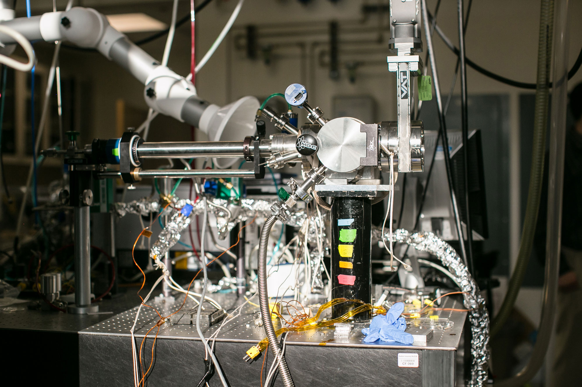
Research Area: Area Selective Atomic Layer Deposition
Modern nanoscale device fabrication schemes rely on a series of 'top-down' steps to produce devices with nanoscale features. However, edge-placement error of multilayered materials is often a significant problem with this type of growth process. Our group studies how unique surface treatment or chemically-selective inhibitor molecules can deactivate some areas of a substrate while allowing material growth on other areas to achieve area selective deposition.
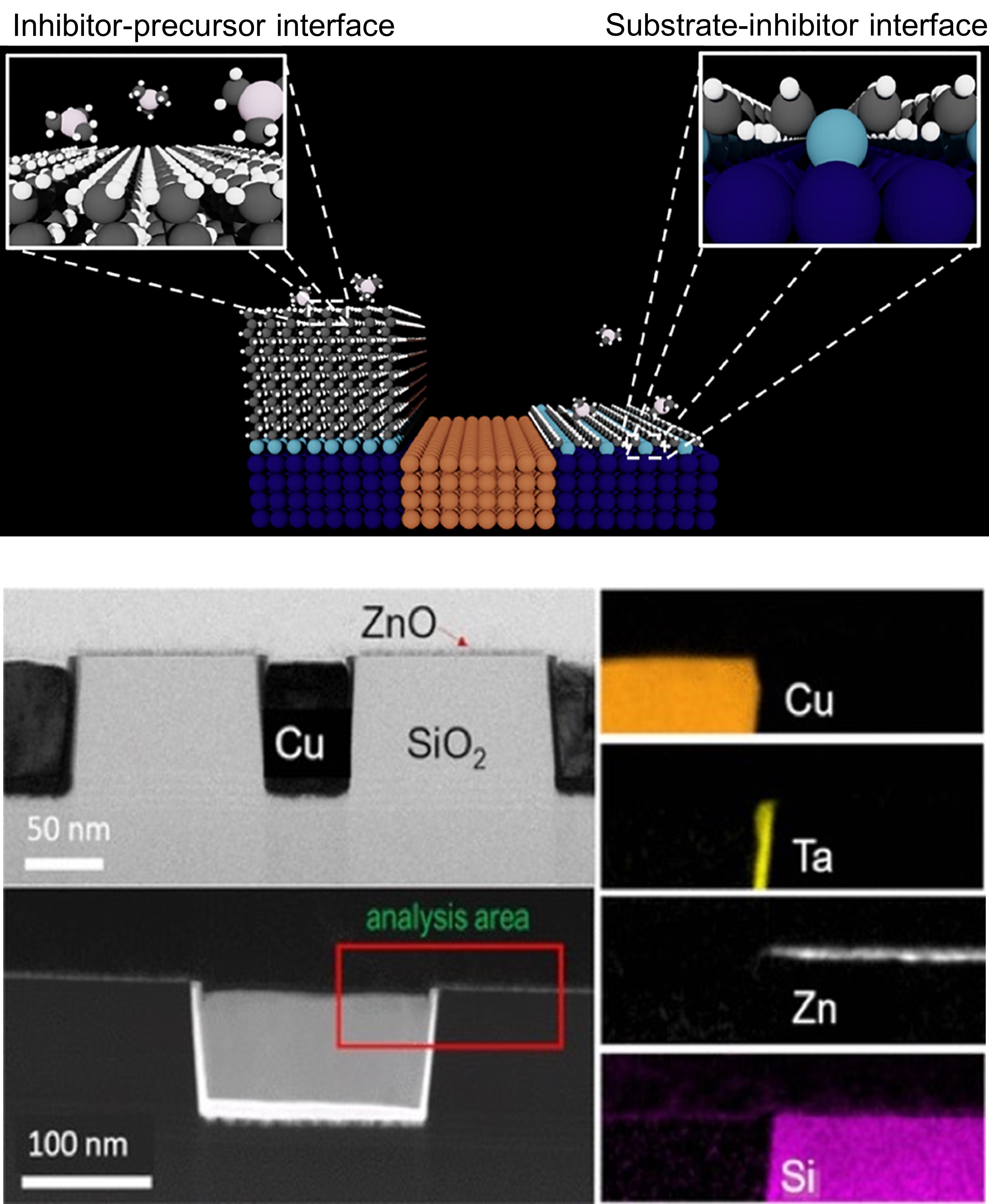
Top: Schematic of area-selective ALD using long chain self assembled monolayer (SAM) inhibitors (left) or small molecule inhibitors (right) chemisorbed to a silica substrate, leaving a bare copper intermediary region Bottom: Cross-sectional TEM, EELS, and EDS spectral images of the monolayer DDT-coated Cu/SiO2 patterns after 15 cycles of ZnO ALD.
Whereas ALD inherently provides nanoscale control of materials in the vertical direction, area selective ALD enables nanoscale definition of the lateral structure. In area selective ALD, we attach inhibitory molecules such as self-assembled monolayers to regions of the substrate to prevent ALD. We can achieve area selective ALD of a range of deposited materials onto metal, semiconductor, and dielectric substrates. By tuning this pre-growth step, in addition to optimizing the ALD process that follows, we can facilitate the selective growth of materials in desired growth areas.
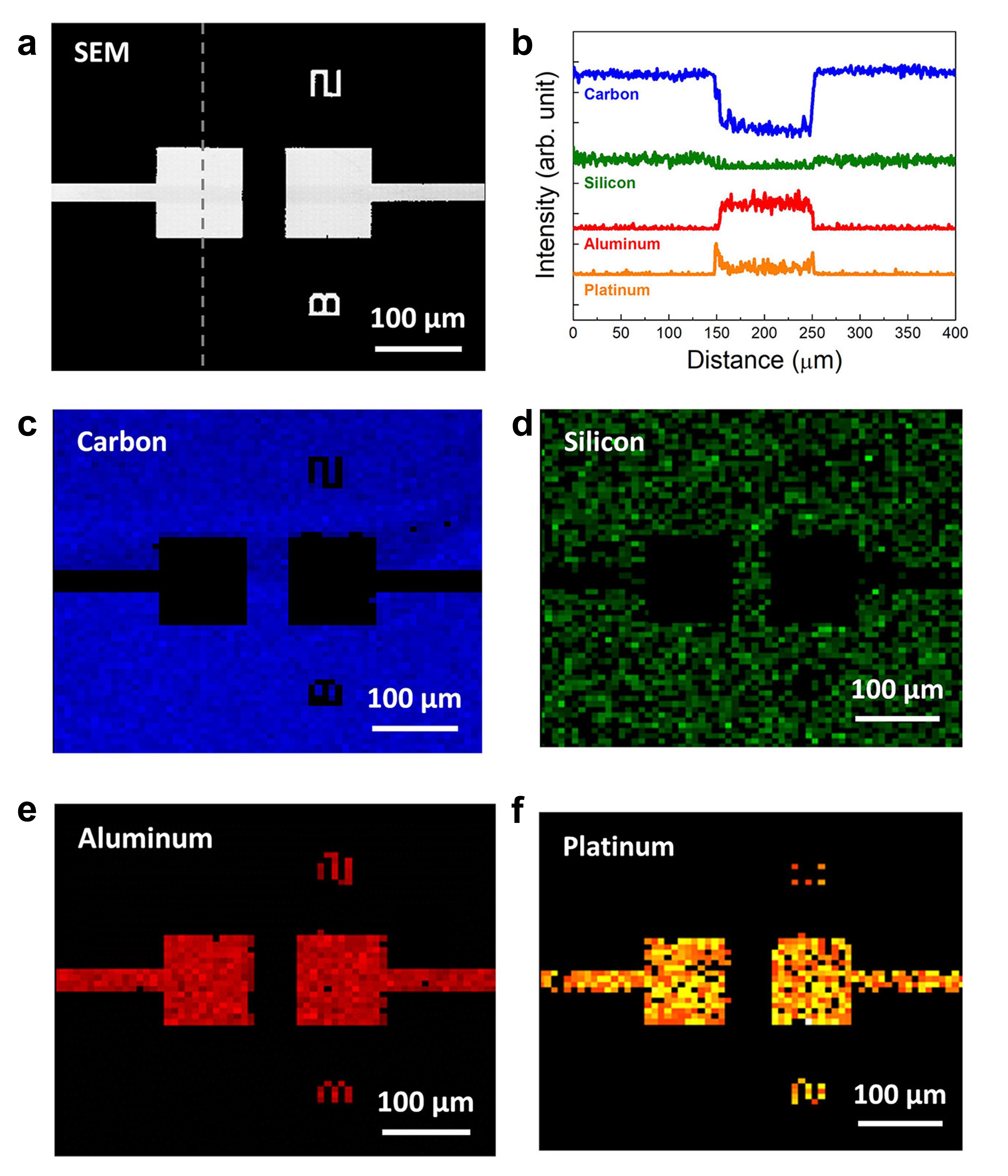
(a) SEM image of 50 cycles of Al2O3 with Al(C2H5)3 on ODTS-treated Pt/SiO2 patterns. (b) Along the vertical dashed line denoted in (a), elemental line spectra for carbon, silicon, aluminum, and platinum. Elemental mapping of AES for (c) C, (d) Si, (e) Al, and (f) Pt.