Research Area: Atomic Layer Deposition
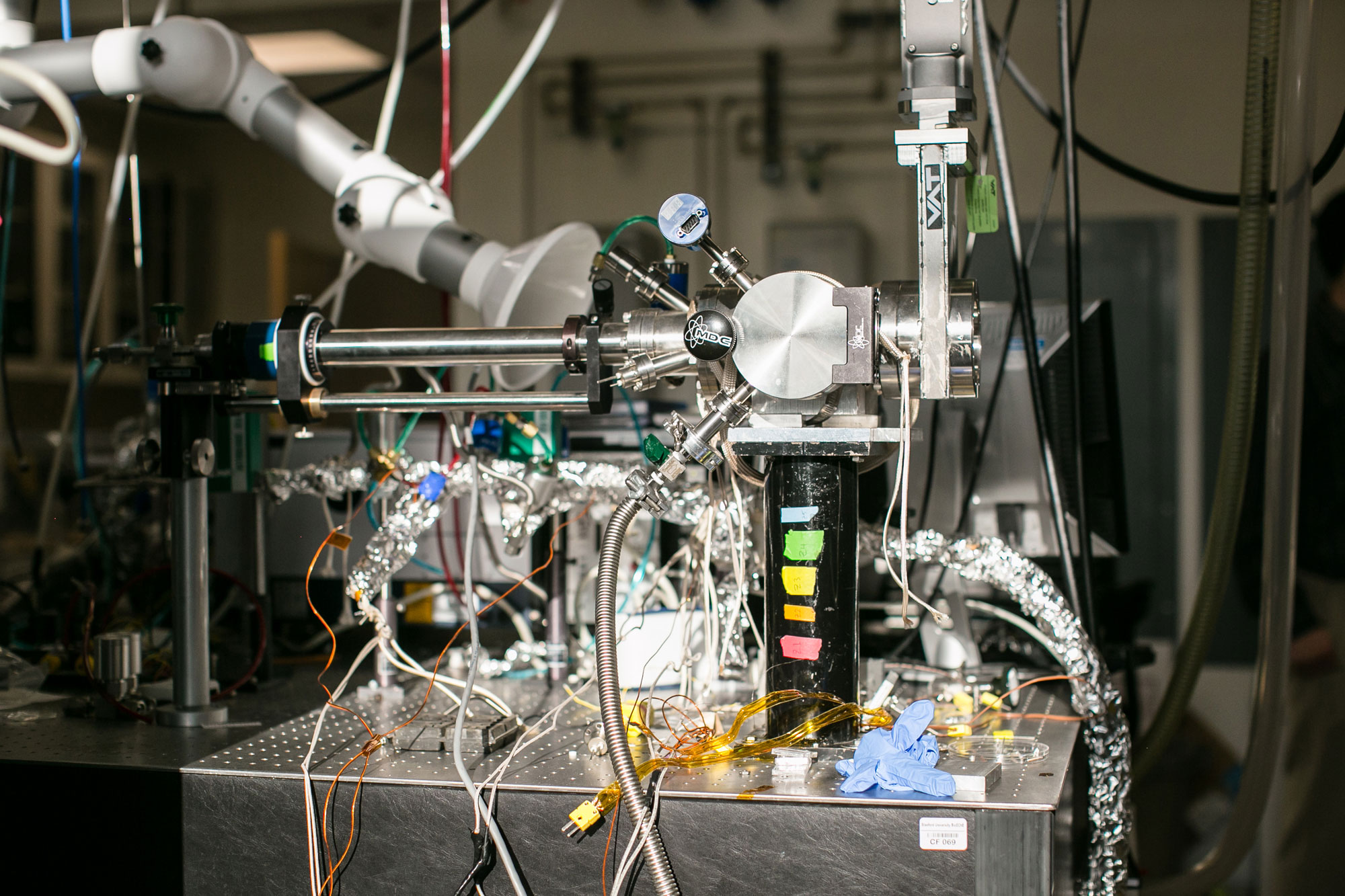
Atomic layer deposition (ALD) is a technique that can be used to deposit thin films with control over the thickness and composition and with an excellent uniformity on 3-dimensional surfaces. Our group studies ALD of a range of materials, including metals, oxides, and sulfides for various applications in nanoelectronics and sustainable energy. We carry out in situ studies of the initial stages of ALD to elucidate the mechanisms of film nucleation and growth using a combination of laboratory- and synchrotron-based experiments and theory. The combination of several different in situ techniques is required to obtain a complete picture of ALD reaction mechanisms.
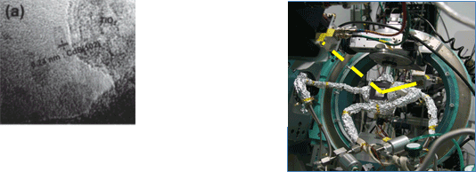
Left: CdS quantum dots deposited by ALD on a TiO2 support. Right: In-situ XRD reactor installed on beamline 7-2 at the Stanford synchrotron radiation lightsource (SSRL).
In addition, our group investigates area-selective ALD. Whereas ALD inherently provides nano-scale control of materials in the vertical direction, area-selective ALD enables nano-scale definition of the lateral structure. In area selective ALD, we attach inhibitory molecules such as self-assembled monolayers to regions of the substrate to prevent ALD. We can achieve area selective ALD of a range of deposited materials onto metal, semiconductor, and dielectric substrates.
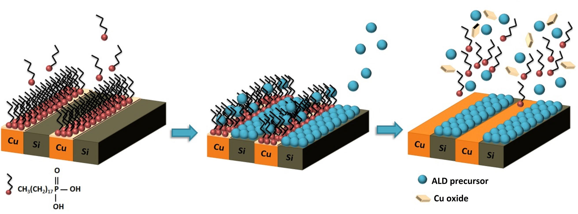
Schematic of area-selective ALD.